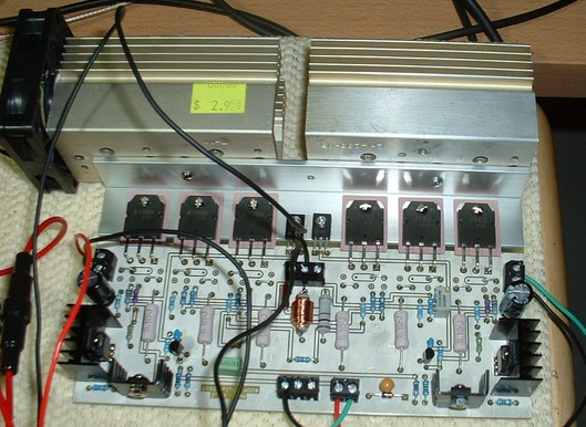
Click on the image below for a full size view of the assembled EC-OPS board. The heatsinks in the picture are for evaluation/testing purposes only.
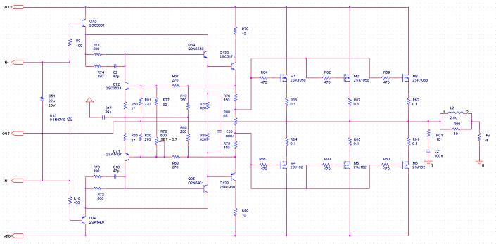
The Error Correction Output Power Stage (EC OPS) is based on Bob Cordells design, which in turn is based on prof. Hawksword breakthrough article in the early 80s. Our implementation allows for either lateral MOSFETs, vertical MOSFET or BJTs. For the reasons detailed here we opted for lateral MOSFETs, but vertical MOSFETs (Fairchild FQA19N20/FQA12P20) and BJTs (2SC5200/2SA1943) were also experimented with good results.
We will not give details here for anything else but lateral MOSFETs output devices. Enough to know that adapting for verticals or BJT involves three steps:
1. Strap the PCB for the correct output device pin-out
2. Adjust the R75/R76/R88 voltage divider for the power devices bias (Note 1 below). Fine adjustments can be done via R78
3. Choose the gate/base resistor. Vertical MOSFETs need lower values while BJTs need even lower values (if at all!).
4. Adjust the Hawksword balance (either R71/R72 or R81/R20) for a minimum in THD. On the Hawksword balance adjustment see Note 2 below.
Click on the image below to get the full size EC OPS electrical schematic.
Note1: For the best results, every active device except for the output transistors should run in Class A. That is, the bias should be chosen such as to avoid saturation or blocking, at all input levels before clipping. This poses some difficulties for a BJT output stage where (to stay in Class A) the drivers stage collector currents should exceed the output BJT base current at maximum output current (that is in our case some 10A). Therefore, the whole bias schema should be redesigned, to allow room for the output BJT base current swing. Also, under these circumstances, the power dissipation in the drivers will be considerable and it is questionable if an onboard heatsink (as included in our lateral MOSFET design) will help if the maximum power of 200W into 4 ohm is targeted. It is therefore reasonable to assume that a power BJT design based on our implementation can not exceed a target of 50W/8ohm and 100W/4ohm. Of course, for such relatively modest power levels, there is no need to install three pairs of output devices, one pair of (e.g.) MJL4281/MJL4302 or equivalent will do the job.
Note2: Adjusting the Hawksword balance requires a dual helipot (at least ten turns) with better than 0.5% matching between sections. We replaced R20 and R81 with a 2K Bourns 10 turns helipot and adjusted for a minimum of open loop distortions at 20KHz. You will find that the minimum is strongly frequency dependent; always adjust for a minimum at the higher frequencies in the audio band. At lower frequencies, the high feedback loop gain will help in lowering the THD levels. Measure and replace the helipot values with fixed resistors. The minimum is usually very narrow so you may need 0.5% or better precision resistors. The target should be to bring the open loop THD-20 at under 0.01% at 10 Veff input level. We built so far four EC OPS boards and got the final open loop THD-20 values at 0.0065%, 0.0075%, 0.0090% and 0.012% (for this last one, we were unable to source precision resistors of the required values).
The output Zobel network is mandatory for the whole amp stability. For the same reasons, the output coil shoud not be under 2uH air core.
The error amplifier frequency compensation C17 is connected to the signal ground of the whole amp, rather than to the power ground. This is for stability reasons and for providing a shielding ground for the feedback connection (the OUT terminal).
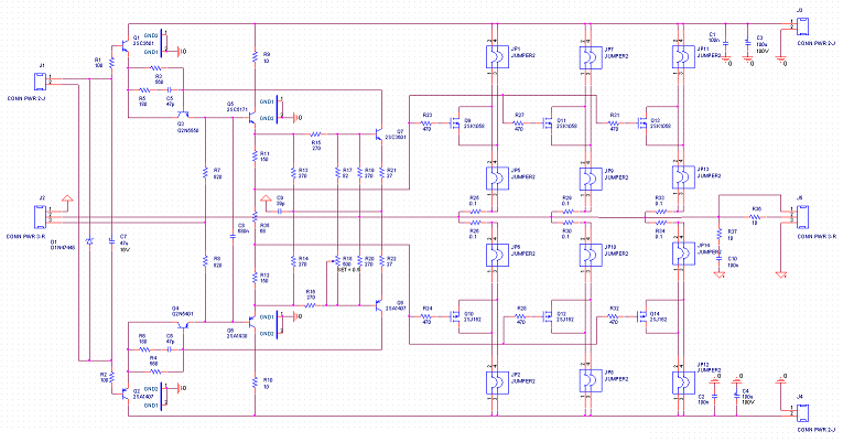
Click on the image below to get the full size EC OPS PCB schematic. You can download all schematics here.
The inputs and outputs are provided via terminal blocks, while the straps allow swapping the source/emitter and drain/collector terminals, to allow for different output device pinouts. The output coil is not figured here, as it is wound around R36. The Zobel resistors should be 5W.
The source 0.1ohm/3W source resistors are metal oxide; we found these better to regular wire wound resistors (having higher parasitic inductances). All other resistors are 0.25W 1% metal film.
Compensation capacitors are ceramic NP0, decoupling and Zobel are metal stacked. Regular electrolytic are used for decoupling.
All onboard heatsinks are connected to the power ground. The differential error amplifier pair is mounted on the same heatsink with the output devices. While this is not required for lateral MOSFETs (they have a negative temperature coefficient of the drain current over some 150mA) it is required for vertical MOSFETs to stabilize the bias. For lateral MOSFETs the differential pair can be mounted vertically, avoiding the direct contact with the heatsink; we though found experimentally no performance impact of the heatsink mount version, as long as the bias current is set to around the equilibrium point of 150mA.
The output devices are mounted on a piece of 1/8 aluminum corner, that is attached to the main heatsink.
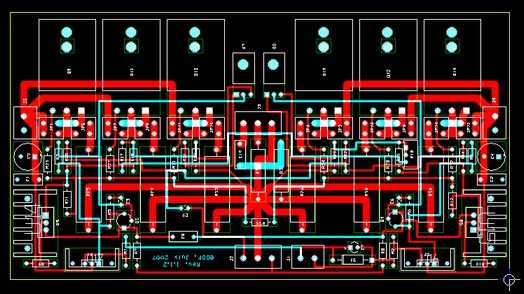
Click on the image below for a full size view of the EC-OPS PCB design (ground plane is removed). Gerber files can be downloaded here
From Genesis to Revelation
The Ultimate Audio Amp
From Genesis to Revelation
The Error Correction Output Stage